Scanning electron microscopy
Scanning electron microscopy (SEM) is a precise and fast technique for studying the microscopic structures and topology of a material’s surface. SEM has numerous applications in research and product development, such as imaging the surface morphology of particles and coatings. Because of its flexibility, SEM analysis can be used to solve a range of problems in the production process.
Take a look at our SEM services
SEM imaging
SEM-EDX imaging of surfaces
Particle size distribution with SEM
Cross-section SEM imaging + Broad Ion Beam (BIB) preparation
Cross-section SEM imaging + Focused Ion Beam (FIB) preparation
Cross-section SEM imaging + freeze fracturing preparation
Particle size distribution analysis according to EC recommendations
Cross-section SEM-EDX imaging + Broad Ion Beam (BIB) preparation
Prices excluding VAT (24 %).
- Fast turnaround times
- Personal service from method experts
- Competitive prices
- Result accuracy guarantee
What is SEM analysis used for?
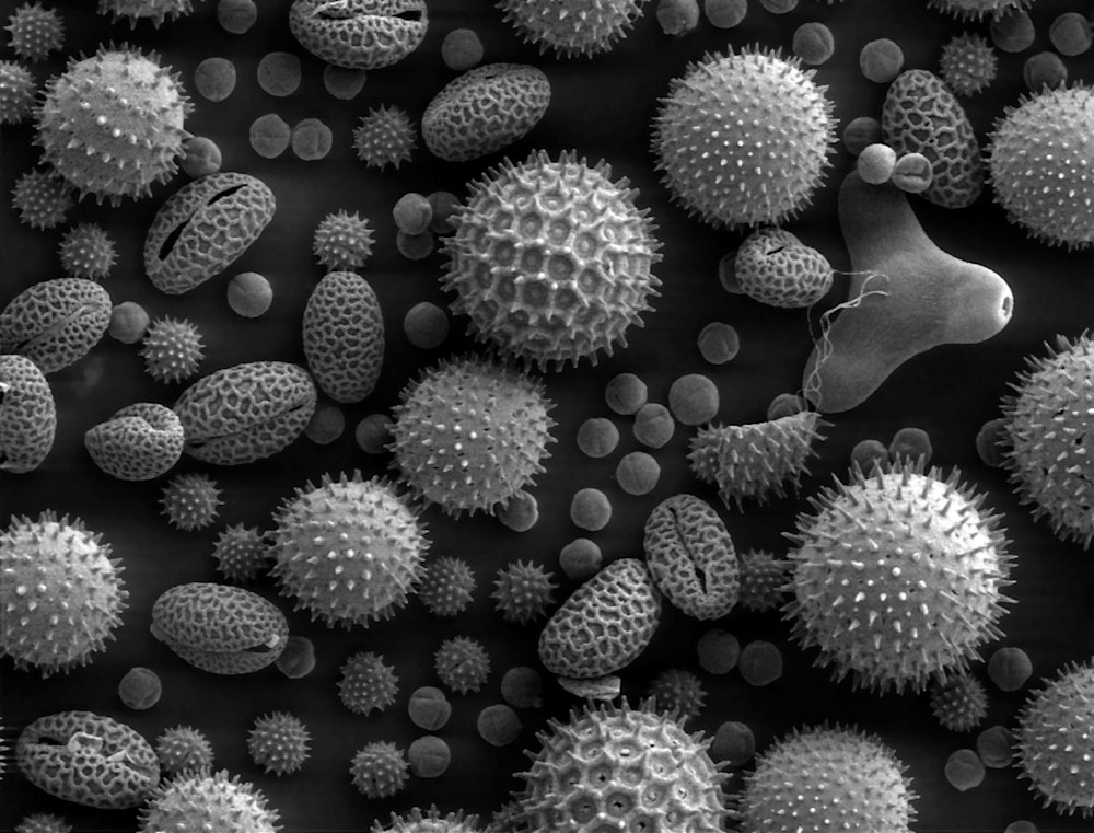
With SEM, the detailed surface structures of the sample can be seen with high accuracy, which means that a precise image of its surface morphology and even topography can be obtained. Some scanning electron microscopes can have a resolution of less than 1 nm, although a resolution of around 1 to 20 nm is more common.
SEM imaging can be used to identify product defects and imperfections in various types of dry solid materials, including thin films, coatings, and construction materials. SEM may also be used to analyze powders and other particulate matter and can provide the particle size distribution of non-spherical particles, like rods and fibers, that are tricky to analyze with conventional methods.
How does SEM work?
In SEM, a beam of electrons systematically wipes the sample's surface. Electrons are accelerated from a source of electrons and directed through multiple electromagnetic lenses and apertures before hitting the sample. The electrons interact with the surface of the sample and produce different signals when they deviate from their original direction. After the interaction has happened, an electron detector detects the electrons, and the information is turned into a picture by a computer connected to the detector.


Additional detectors
There are many different SEM setups, additional detectors, and techniques available for different demands. SEM can be combined with EDX (energy-dispersive X-ray spectroscopy) to perform SEM-EDX analysis. With this method combination, it is possible to determine the elemental composition of the sample in addition to its surface structures. Another possible addition is the electron backscatter diffraction (EBSD) detector, which can be used to visualize the microstructure of crystalline samples.
Suitable samples
Samples used in SEM must be dry, and their surfaces must conduct electricity. If this is not the case (for example, with biological samples), they must be pretreated before SEM. Usually, samples that do not conduct electricity must be coated with a conducting material. Suitable coatings include platinum, gold, palladium, and carbon.
SEM vs. traditional microscopy
The resolution of a picture taken with a microscope - that is, the shortest possible distance between two different targets with which the targets can still be distinguished from each other - depends on the wavelength of the electromagnetic radiation (for example light).
Because electrons have a shorter wavelength than photons, electrons can be used instead of light to get a higher resolution. Therefore, the smallest details of the sample can be seen more closely with an electron microscope than with a traditional optical microscope. If an even higher resolution is needed, transmission electron microscopy (TEM) may be used.
Need an analysis?
Measurlabs offers SEM analyses for various industries and analytical purposes. Some popular applications include failure analysis of semiconductors and determining whether food products contain nanoparticles, but these are just examples. Do not hesitate to contact us through the form below to discuss your testing needs.
Suitable sample matrices
- Solid samples
- Powders
- Metals
- Polymers
Ideal uses of SEM
- Product development and quality control, for example failure analyses
- Material examination, for instance observation and measurement of the tiny detailed structures of the material’s surface and analysis of its breaking mechanisms
- Study of complex environmental and biological samples to find out the microscopic structures of their surfaces
Ask for an offer
Fill in the form, and we'll reply in one business day.
Have questions or need help? Email us at info@measurlabs.com or call +358 50 336 6128.
Frequently asked questions
Scanning electron microscopy is commonly used to screen solid surfaces for cracks or impurities, detect nanoparticles in food samples, and analyze the thickness of semiconductive thin films. SEM can also be used for particle size distribution analysis, where its advantage is the ability to detect particle shape as well as size.
In the SEM-EDX method, an EDX detector (also called EDS) is connected to a standard SEM machine. SEM-EDX can be used for identifying elements and determining their distribution and concentrations in the sample. When electrons interact with the surface of the sample, they make the sample produce X-rays which can be detected with an EDX detector. Because every element has its own kind of X-ray spectrum, the elements and compounds in the sample along with their concentrations can be discovered with SEM-EDX.
In addition to EDX, an X-ray detector (XRF) can identify elements even to the nearest micrometer based on their X-ray spectra when used together with SEM.
With SEM, only the surface structures of the sample can be examined. Even though cross-sectioning of the sample can be used to see the inner structures, this method is not an option if the sample and its inner parts are to be kept in one piece and undamaged. In such cases, non-destructive alternatives like micro-CT imaging may be preferable.
If the sample is too large for the microscope, it may need to be cut before the analysis. This is often done using focused ion beam technology. Other sample preparation techniques are usually needed if the sample is dirty, wet, or does not conduct electricity.
The elements present on the surface of the sample cannot be identified with SEM alone. Instead, SEM-EDX and XRF are suitable methods for this purpose.
Solid samples are suitable for SEM analysis. Samples must be dry and their surfaces electricity-conducting for most SEM techniques to work. If the sample does not meet these requirements, it must be pretreated before imaging.
Measurlabs offers a variety of laboratory analyses for product developers and quality managers. We perform some of the analyses in our own lab, but mostly we outsource them to carefully selected partner laboratories. This way we can send each sample to the lab that is best suited for the purpose, and offer high-quality analyses with more than a thousand different methods to our clients.
When you contact us through our contact form or by email, one of our specialists will take ownership of your case and answer your query. You get an offer with all the necessary details about the analysis, and can send your samples to the indicated address. We will then take care of sending your samples to the correct laboratories and write a clear report on the results for you.
Samples are usually delivered to our laboratory via courier. Contact us for further details before sending samples.